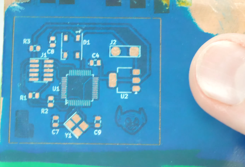
Normally, you have a choice with PCB prototypes: fast or cheap. [Stephen Hawes] has been trying fiber lasers to create PCBs. He’s learned a lot which he shares in the video below. Very good-looking singled-sided boards take just a few minutes. Fiber lasers are not cheap but they are within range for well-off hackers and certainly possible for a well-funded hackerspace.
One thing that’s important is to use FR1 phenolic substrate instead of the more common FR4. FR4 uses epoxy which will probably produce some toxic fumes under the laser.
We were surprised at how good the boards looked. Of course, the line definition was amazing, as you’d expect from a laser with details down to 200 microns (a little less than 0.008″), and he thinks it can go even lower. The laser also drills holes and can cut the board outline. A silk screen makes it easy to add a solder mask, and the laser will even cut the mask. [Stephen] also etched “silk screening” into the solder mask and filled it with a different color solder mask to make nice board legends.
Registration is critical and will be extra critical for two-sided boards which is what he’s working on now. We think if you put some scored carrier edges around the board with fiducials, you could make a jig that would hold the board in a very precise position using the holes in the carrier edges.
Vias are another issue. He mentions using rivets, but we’ve also seen people simply solder both sides of a wire through a hole, which isn’t that hard.
For most people, making your own PCBs is fun but not very practical. But there is something about being able to turn around actually good-looking boards multiple times in a day when you are doing heavy development. If you don’t mind fumes, you can laser mark your PCBs.