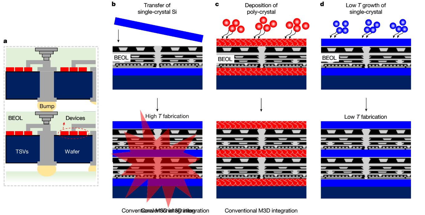
 paper in Nature by [Ki Seok Kim] and colleagues (gift article), this technique of monolithic 3D (M3D) integration required overcoming a number of technological challenges, most of all enabling the new TMD single-crystals to grow at low enough temperatures that it doesn’t destroy the previously created circuitry. The progress is detailed in the paper’s schematic (pictured above): from TSV to M3D by transfer of layers and high- and low-temperature growth of single-crystal layers.
Ultimately, the demonstration device with vertically grown transistor arrays (nMOS and pMOS) on a silicon substrate was grown at 385℃, which, if commercially developed, could mean a significant boost in transistor density and possibly the development of 3D semiconductor circuits rather than stacked 2D ones. We are still worried about making them the old-fashioned way.